
Exploring the PCIe Bus Routes
As is evident from the Cirrascale web page, we do a lot business with customers making use of GPU Compute (or other computational accelerators, such as the Intel® Xeon Phi™ Coprocessor). While a few of our customers have workloads that are embarrassingly parallel, most applications require some sort of intercommunication between GPUs, so understanding the data flow between GPUs is important for getting optimal performance out of the system. Even for the embarrassingly parallel jobs, getting data to the GPUs to keep them busy requires understanding the inter-system flow of data between local and remote systems.
Many of the people I talk to about GPU Compute are familiar with the typical 8 GPU systems on the market today, such as the Tyan FT77AB7059 or Supermicro 4027GR, which make use of 4 PCIe switches, and all PCIe lanes of a dual-socket Intel® Xeon® processor E5-2600 series based server.
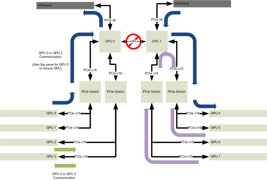
GPUs are divided between the two CPUs, and each pair of GPUs is behind a PCIe switch. This configuration is popular with system vendors because it’s relatively easy to build: keeping PCIe integrity between 3 devices (the PCIe root in the CPU, and the two GPUs on any particular PCIe switch) is relatively easy given the physically short trace lengths that are attainable with this configuration. Unfortunately for users, there are a number of downsides to this configuration.
As illustrated by the green arrows in the picture above, communication between two GPUs on the same switch is straightforward: data from a GPU (GPU 2 in the picture above) goes to the switch, then right back down to the adjacent GPU (GPU 3 in our illustration). Full PCIe x16 bandwidth, and minimal latency for that transaction. Going between two non-adjacent GPUs on the same CPU, illustrated by the purple arrows, induces a bit of extra latency due to the two switches and root complex that packets must traverse, but overall it’s “not that bad”. Using the NVIDIA CUDA 6.0 “p2pBandwidthLatency” sample as a trivial benchmark, there is roughly a 7% bandwidth (9.8 GB/s vs 10.6 GB/s) and 2% latency (7.9μs vs 7.7μs) penalty for the extra complexity in the data path1. On the software front, this is all transparent, with all 4 GPUs being able to peer with each other (to use CUDA parlance), making the writing of multi-GPU software pretty straightforward.
This typical 8 GPU system configuration, where some of the GPUs are on different sockets than the others, also means that there is yet another data-path for getting between GPUs, that of getting from one half of the GPUs (e.g., GPU 0-3) to the other (e.g., GPU 4-7). Here is where things get really ugly. Looking again at the illustration above, consider the case where GPU 0 (on CPU 0) wants to share data with GPU 4 (on CPU 1). The traffic leaving GPU 0 starts like any other transaction, heading first to the local PCIe Switch, and then on to the PCIe Root (CPU 0). But where does it go next? The logical place would be to make use of the high-bandwidth, low-latency QPI bus between the two CPUs, then to the PCIe Switch, and finally to GPU 4. Unfortunately, that’s a really bad idea, and the reason for the universal “No” symbol around QPI in the illustration above. In current generations (IvyBridge) of Intel Xeon processor E5-2600 series CPUs, the generally really useful QPI link introduces significant latency when forwarding PCIe packets between processors due to the way the packets are buffered and forwarded. How big is “significant”? Going back to our NVIDIA® CUDA® 6.0 “p2pBandwidthLatency” test, the 10.6 GB/s bandwidth observed between two GPUs on the same switch drops to a dismal 4.0 GB/s (just 38% of it’s former self!), while latency skyrockets from 7.7μs to an astronomical 32.1μs (a 316% change in the wrong direction)2. If high bandwidth, low latency inter-GPU communication is what you’re after, the QPI link should not be your preferred mode of transportation. There’s also the fact that since half of the GPUs in the system now reside on a different PCIe root (“CPU 1″ vs “CPU 0″), they can’t see the address space of all GPUs, and therefore extra care needs to be taken for writing multi-GPU enabled software. New APIs made available in CUDA 6.0 have gone a long way toward removing much of this complexity, allowing for buffers to be managed by CUDA, but just because CUDA can now take care of moving data between different groups of GPUs doesn’t make the performance impact any less dramatic.
Since QPI is out as a method to get PCIe packets from one set of GPUs to another, a potential solution is to use a low-latency interconnect such as Infiniband. While I’m not personally a fan of Infiniband, it does have it’s place; and that place is when you need really low latencies. Infiniband gives per-packet latencies in the single-digit microseconds3, which ends up matching nicely with what is needed to extend inter-GPU communication. The bonus of using a transport like Infiniband is that it makes no difference if the “other” GPUs are on the socket next door, or on another system elsewhere in the network. Given suitable GPU Direct RDMA capable drivers, this seems like a pretty decent solution, unless you are actually developing applications. In that case, there’s some extra overhead from the users perspective…okay, a lot of extra overhead, as now any application that wants to use a non-trivial number of GPUs needs to start getting involved in the job scheduling business, and have knowledge that some traffic needs to take a different transport (Infiniband) than others (PCIe). Going back to the typical 8 GPU system shown above, there’s also the fact that the Infiniband connectivity to GPUs is only PCIe x8. More than sufficient for a single FDR port (56Gbps), but significantly less than what GPUs on the same PCIe root complex can achieve when talking amongst themselves.
Unfortunately, this is where many people I talk to have stopped. They have the notion that “Yes, you can put 8 GPUs in a server,” accompanied by a huge caveat of “but it won’t perform like you’d want”. Fortunately, “typical” isn’t what we do at Cirrascale, so I get to talk about changing expectations of how a GPU heavy system behaves.
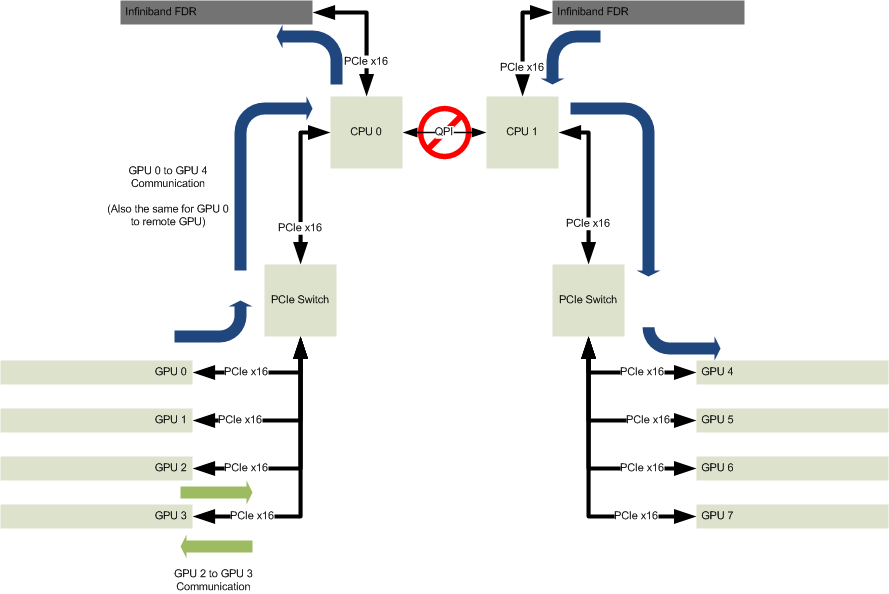
The Cirrascale GB5470 is a flexible platform allowing us to support a number of different PCIe topologies. The most logical evolution from the typical 8 GPU system is what is shown in the diagram above. This configuration improves on two of the problem areas discussed above. First, instead of using 2 GPUs behind a switch, 4 GPUs are now placed on the same switch (using the Cirrascale PCIe Gen3 Riser), removing the additional PCIe latency induced by the prior configuration in some scenarios. The green arrows showing communication between GPU 2 and 3 could apply to any pair of GPUs on that same CPU socket. This allows more freedom for users, as the traffic pattern between GPUs can be handled at run-time not system-build time. Applications can decide to pair up any GPU 0 through 3 with any other GPU 0 through 3, as the bandwidth and latency between any two is identical. Similarly, if an application requires communicating with more than one GPU, there are 3 others to choose from with no penalty. The second significant improvement is for communicating between sets of GPUs on different sockets, shown by the blue arrows. The Infiniband (or whatever the interconnect of choice is…our GB5470 doesn’t really care what you use, and we’ve seen some crazy things!) now has a full PCIe Gen3 x16 connection, allowing for something like an Infiniband dual-port FDR card (such as the Mellanox MCB194A-FCAT) to be used for inter-GPU communication. If a GPU needs (almost) full PCIe Gen3 x16 bandwidth to another GPU, it is now possible.
For many applications, the configuration above is a significant boost in capability over what users are accustomed to. Some applications can make better use of a different PCIe topology in the GB5470, which solves a different set of problems.
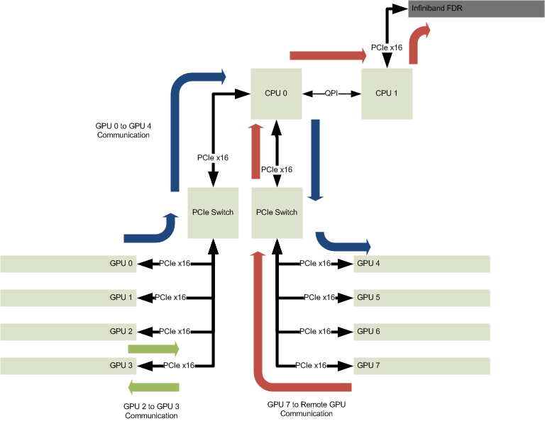
Moving all 8 GPUs to the same PCIe root (“CPU 0″ in the diagram above) is the obvious big win of the configuration shown above. 8 GPUs on the same PCIe root (and hence able to be peers in CUDA terms) makes for a really fast and flexible system. Of course there are still some PCIe topology considerations to keep in mind, like scheduling transfers to GPUs on the “other” PCIe switch so as to not saturate the PCIe Gen3 x16 link to and from the CPU, but for users accustomed to trying to manage two pairs of GPUs in a typical 8 GPU system, the constraints of this configuration are trivial to deal with. The huge benefit here, of course, is that all 8 GPUs share the same address space, and data can be shared between them trivially and transparently using CUDA APIs. The blue arrows showing GPU communication no longer have to go over an Infiniband link, but remain entirely on the same PCIe root: Low latency and high bandwidth for 8 GPUs. A notable downside is that to get data on or off the system, the QPI bus must be used. Since communication between GPUs and the Infiniband card isn’t direct in many applications (there’s oftentimes a bounce-buffer used, if not some higher-level protocol handling with some pointer shuffling, since GPU Direct RDMA isn’t possible here), this doesn’t necessarily hit the QPI performance problems that afflict the configurations mentioned previously (and the Infiniband card is still on a full PCIe Gen3 x16 bus, just on the “other” CPU), but it is clearly not optimal. However for GPU compute jobs which can “fit” within 8 GPUs, this configuration offers unparalleled bandwidth and latency between GPUs. A large number of applications really excel in this configuration due to the relatively flat PCIe topology.
It’s probably obvious that there are a number of other possible configurations for the GB5470, such as replacing one of the GPUs in the previous configuration with the Infiniband card; sacrificing a GPU worth of compute capability in return for exceptionally high bandwidth and low latency inter-system communication. For others applications, where the inter-system communication can be supported with a PCIe Gen3 x8 connection (read: Usually a single-port Infiniband FDR card) and x86 CPU resources aren’t in high demand, single socket solutions make more sense.
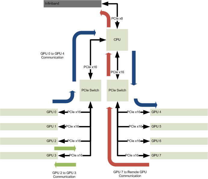
A PCIe topology as shown above (another Cirrascale GB5400-series system, making use of Intel® Xeon® processor E5-1600 series CPUs) yields low latency inter-system communication, while preserving the benefits of 8 GPUs on the same PCIe root complex. There are obviously other tradeoffs involved with this solution, related to the single-socket nature of this product (higher CPU clockspeed, but lower overall core count and RAM volume than a dual-socket system), but that’s why I enjoy talking with people about our products.
Understanding what users are trying to achieve with their GPU intensive applications gives me reason and opportunity to explore what bottlenecks are holding them back. In turn, I can arm them with knowledge that lets us work together to think beyond the typical system, and instead toward what’s possible.
1. Benchmark run on CentOS 6.5 x64 (kernel 2.6.32-431.11.2, NVIDIA driver 331.44, CUDA 6.0RC) using NVIDIA K40 cards and the p2pBandwidthLatency CUDA sample. Measurements are the mean of 5 test runs with P2P enabled unidirectional traffic.↩
2. Benchmark run on the same system as previously described.↩
3. http://www.hpcadvisorycouncil.com/pdf/IB_and_10GigE_in_HPC.pdf↩
Intel, the Intel logo, Xeon, and Intel Inside are trademarks of Intel Corporation in the U.S. and other countries. NVIDIA, Tesla, Quadro, GRID, and GeForce are trademarks or registered trademarks of NVIDIA Corporation in the U.S. and other countries.All other names or marks are property of their respective owners.


- ← Do You Really Get What You Pay For, or is Perception Reality?
- Digital Detox: Take a Break on Vacation →
Hi,
We have embarrassingly parallel CUDA code in genomics/bioinformatics. It looks like the third configuration above would map well to these algorithms. Does that sound right?
Email: info@rmcsoftwareinc.com
Linkedin: http://www.linkedin.com/in/richardcaseyhpc
Blog: rmcsoftwareinc.wordpress.com
Twitter: @rmcsoftwareinc
Facebook: http://www.facebook.com/richardcaseyhpc
Google+: plus.google.com/107594981582657849119/posts
Technically if it’s embarrassingly parallel, then the 1st configuration (the “Typical 8 GPU Server”) would make the most sense. That’d let you move code H2D/D2H while having to put minimal thought into scheduling those copies to minimize bandwidth bottlenecks. It does preclude you from taking real advantage of D2D (“P2P” in NVIDIA parlance) transfers though, which isn’t terribly forward looking.
Practically, genomics workloads are moving toward data flows where the the 2nd or 3rd configuration makes the most sense. From a Cirrascale product standpoint, I see people buying a GB5470 configured like the 2nd configuration (4x cards on each of two CPUs), and converting that to the 3rd configuration (8x cards on one CPU) for their leading-edge developers.
Nice article and thanks for the QPI results. Any update on bandwidth / latency improvements with a pair of E5-2600 V2s in the same backplane, or better yet, V3s in 2011-V3s w/C612?
Hi Scott,
Sorry, I missed this comment! I don’t usually ignore things for 4 months!
The 2011-3 processors (E5-2600v3 series) don’t seem markedly different in our testing regarding passing PCIe frames across the QPI link. I expected there to be some improvements (since the buffer sizes changed), but initial testing doesn’t show a dramatic improvement with the p2pBandwidthLatency tool. I have on my to-do list an update to the benchmarks (along with CUDA 7 or better), but seems it never makes it’s way to the top of that list.
What I do find interesting through is that more recent NVIDIA drivers (and/or CUDA 7, not entirely sure which yet) have started to do a darned good job masking the QPI latency, so larger transfers (not the 1-byte cudaMemcpy() that the p2pBandwidthLatency test does) can get pretty close to maximum bandwidth across the QPI link. Latency is still horrible, of course, but if you ask CUDA to move a lot of bits from one side of the QPI link to the other, you can achieve respectable goodput numbers.
Well technically PLX Tech has an off-the-shelf PCIe switch. It just is off the shelf and onto a custom PCB with some firmware and ancillary logic, not right into a PCIe slot.
I can see it being a small-ish market, but it’s odd to me that even PLX Tech’s top-end part stops at 96 PCIe lanes. Once you’ve got the logic built for a switch, I’m not sure why there wouldn’t be a choose-your-own-number type of product matrix, from 32 to 256 (or some other absurd number). Especially given the flexibility of doing (effectively) VLANs on the part, having a bucket-full of lanes, rather than only 80 or 96, would seem logical.
We’re working on getting a closer relationship with PLX Tech (and similar companies) to help further this, and other ideas, to help drive the HPC market forward.
I’ve a little surprised that nobody has come out with a off the shelf PCIe crossbar switch.
A few vendors (HP notably) have done their 8 socket servers with a custom QPI crossbar and their Superdome servers use a proprietary I/O crossbar. Ideally you’d have something like a dual-root (so you could hang off both CPUs) with on-chip cut-through.
One interesting question is are you bandwidth bound at all, ie: do you really utilize the x16 bandwidth?
For 8 x16 slots plus the two root ports that’s about 800 signal lines. You could almost do this on a single FPGA with some trickery at x16…at x8 it would become easier. The limiting factor in current top of the line FPGAs is the number of high speed serial transceivers and the limitation of the canned PCIe logic blocks to x8. It would also be possible to do it pretty easily with two FPGAs utilizing a cut-through to a bus…that would have an advantage of working into existing designs fairly easily (one root and 4 slaves per FPGA). All that being said it’s still surprising somebody hasn’t spun an ASIC…the demand seems to be there. Not that it would be a huge volume part…